


RESEARCH
Advancing Dielectric Film Technologies for Ultra-Low-Loss Wide-Bandgap Semiconductor Power Devices
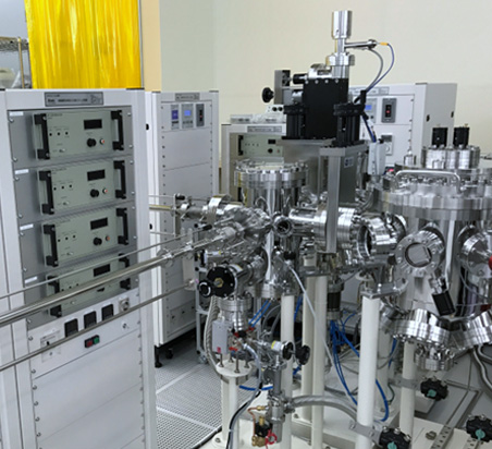
The energy crisis stands as one of the most pressing challenges of the 21st century, and addressing it requires significant advancements in the performance of power devices that govern the transport and conversion of electrical energy. Wide-bandgap semiconductors such as silicon carbide (SiC), gallium nitride (GaN), and gallium oxide (Ga₂O₃) are emerging as next-generation materials capable of surpassing the theoretical limitations of conventional silicon-based power devices. These materials offer the potential for device miniaturization and substantial energy savings. Our research focuses on the development of metal-oxide-semiconductor (MOS) power devices, which serve as the cornerstone of modern switching technologies. In particular, we are investigating optimal dielectric film formation processes through atomic-scale control of surface and interface reactions, aiming to realize high-performance, highly reliable MOS devices.
Quantum Technologies Based on Single-Photon Sources and Spin Defects in Semiconductors
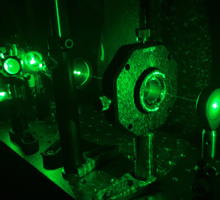
Quantum communication with complete confidentiality and quantum computing capable of ultra-fast processing are anticipated to be transformative technologies that will shape future society. Central to these advancements are single-photon sources and spin defects, which originate from imperfections in wide-bandgap semiconductors. A prominent example is the nitrogen-vacancy (NV) center in diamond, widely studied for its ability to preserve quantum states even at room temperature. With an eye toward the practical implementation and integration of quantum devices, our research focuses on developing promising defect systems in silicon carbide (SiC), a material supported by mature crystal growth, processing, and device fabrication technologies. Specifically, we aim to construct unconventional devices grounded in the fundamental principles of quantum mechanics by establishing methods for defect formation and enabling flexible control over their luminescence and spin properties.
Low-Power Optoelectronic Fusion Devices Based on Group IV Mixed Semiconductors
As digitalization and the proliferation of the Internet of Things (IoT) accelerate, existing information and communication systems are approaching their limits in transmission speed and processing capacity. The fusion of electronics and photonics is emerging as a transformative technological innovation to overcome these constraints. By integrating optical and electronic devices, it becomes possible to significantly enhance data transmission speeds while achieving ultra-low power consumption. This integration also opens new frontiers in quantum information technology, biosensing, and ultra-high-speed image sensing. Our research focuses on the development of optoelectronic fusion devices based on group IV materials such as germanium (Ge) and germanium tin (GeSn), aiming to realize a true convergence of electronics and photonics.
Elucidating Spin and Optical Properties of Semiconductor Defects via Supercomputer Simulations
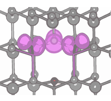
Defects in semiconductor materials—such as substitutional atoms and vacancies—play critical roles as dopants, carrier traps, and recombination centers, fundamentally influencing the performance of electronic and optical devices. Beyond these conventional roles, certain defects also function as single-photon emitters and spin-based quantum light sources, making them highly attractive for applications in quantum computing. Achieving flexible formation, control, and manipulation of such defects requires a deep understanding of their microscopic structures, as well as their spin and optical properties. To this end, we are investigating the physical characteristics of defects by modeling the interactions between nuclei and electrons using ab-initio calculations on supercomputers. Our goal is to generate insights directly applicable to materials and device design, with a particular focus on defects in wide-bandgap semiconductors and at insulator/semiconductor interfaces.